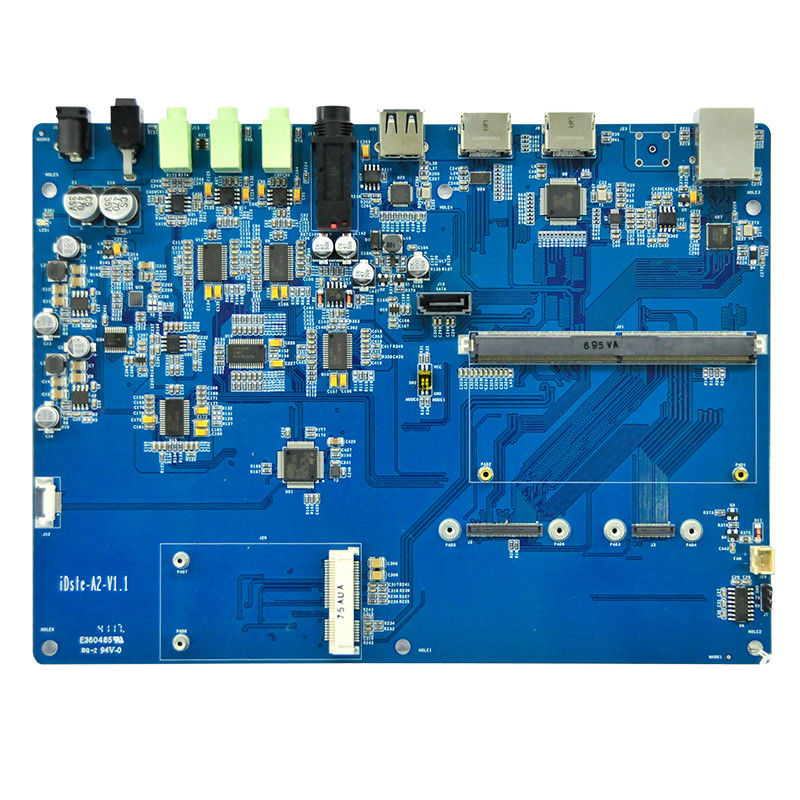
2.0mm 10 Layer HDI Electronic Circuit Board High Frequency PCB Plugged Vias
Founded in 1998, Linked Electronics is now one of the leading one stop PCB solution provider in China.
We have great advantage in the fabrication of high mix, high precision, high end and quick turn PCB board, and rigid flex boards.
Following Services Can be Provided by Linked Electronics
1)1-32 layers PCB board
2)HDI Blind&Buried holes multilayers PCB board
3)High frequency special material base PCB board, such as Rogers, Taconic, Arlon, etc.
4)Heavy copper PCB boards, impedance control circuit boards, carbon ink or peelable mask PCB
5)Assembly Processing: SMT, COB, THT
6)Testing Methods: Flying Probe Test, X-ray, ICT and AOI.
High-density interconnect (HDI) printed circuit boards (PCB) plays an very important role in electronics industry. With the development of 5G and IoT, more and more electronics design engineer use HDI PCB, because the advantages are obvious.
1. Longer battery life due to decreased power usage.
2. Electronics products is getting smaller because more componenents could be populated on both sides
of the HDI PCB by Linked Electronics.
3. If BGA and QFP package is used, Linked Electronics advise the designer to use HDI PCB, because it is more reliable in transmission. HDI by Linked Electronics can accommodate more dense QNF and BGA than previous technique.
Product type: 10 Layer HDI PCB
Application: Communication Industry

| CAPABILITY |
STANDARD |
ADVANCED |
| MinimumLayer Count |
1 |
1 |
| Maximum Layer Count |
12 |
32 |
| Material |
FR-4 (Tg-135C, 145C, 170C), Halogen- free
Rogers Ultralam 2000, Rogers RO4350, Rogers RO4003
Polyimide
Teflon
Black FR-4
Arlon AR-350
CEM-3
Getek Copper Clad Thermal Substrates
Hybrid (Rogers and FR4) BT Epoxy
Nelco 4013
PTFE
Metal Core Materials
Aluminum Core
|
| Board Thickness |
0.020"-0.125" |
0.005"-0.250" |
| Maximum Board Size |
16" x 22"
12" x 21"
22" x 28"
|
10" x 16"
16" x 22"
12" x 21"
22" x 28"
|
| Copper Thickness |
0.5 oz – 3 oz |
0.25 oz – 12 oz |
| Minimum Trace Width / Spacing |
0.004"/0.004" |
0.003"/0.003" |
| Solder Mask Color |
Green, Blue, Black, Red, Yellow, White, Clear, and customized |
| Silkscreen Color |
White, Black, Yellow, Green, Red, Blue and customized |
| Minimum Hole Size |
0.008" |
0.004" |
| Finished Hole Size Tolerance |
+/-0.003" |
+/-0.002" |
| PCB Surface Finish |
HASL (vertical & Horizontal), Lead Free HASL, OSP/Entek, ENIG, ENEPIG,
HASL + Gold Finger,Immersion Tin(ISn), Immersion Silver(IAg), Carbon
Ink, Hard Gold(Flash Gold), Soft Gold
|
| IPC Class |
Class 2 |
Class 3 |
| Controlled Impedance Tolerance |
+/-10 % |
+/-5 % |
| Blind Vias |
Yes |
Yes |
| Buried Vias |
Yes |
Yes |
| Aspect Ratio |
8/1 |
15/1 |
| Minimum Core Thickness |
0.004" |
0.002" |
| Carbon Ink |
Yes |
Yes |
| Peelable Mask |
Yes |
Yes |
| Solder Sample |
Yes |
Yes |
| First Article |
Yes |
Yes |
| ISO 9001: 2008 |
Yes |
Yes |
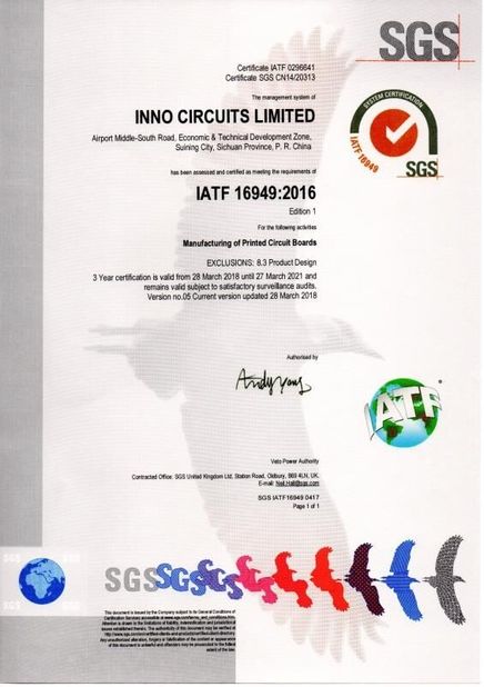
| ISO/TS16949: 2009 |
Yes |
Yes |
| UL 94v0 |
Yes |
Yes |
Technique for PCB Assembly by Linked Electronics
1).Professional surface mounting and through hole soldering technology;
2).Various sizes,like 1206,0805,0603 components SMT technology;
3).ICT(In Circuit Test),FCT(Functional Circuit Test) technology;
4).Nitrogen gas reflow soldering technology for SMT;
5).High standard SMT&Solder Assembly line;
6).High density interconnected board placement technology capacity.
Information Required for RFQ
1).The detailed files(Gerber files,specification and BOM);
2).Clear 3D pictures of PCBA or samples for us;
3).Test Method
 Your message must be between 20-3,000 characters!