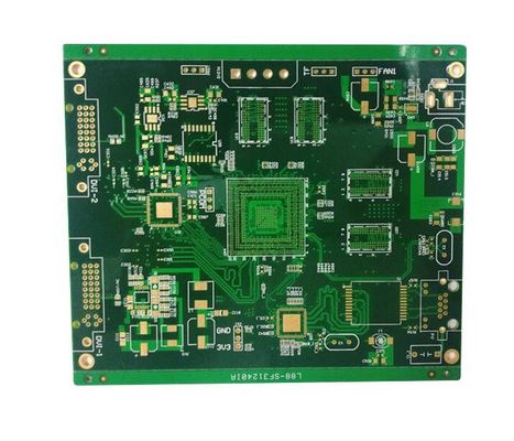
Quick Turn PCB Reliable Electronic PCB Assembly SMT PCBA Assembly Sevice
Linked Electronics is a China based PCB and PCBA manufacturer which specialized in high-mix, prototype, low volume and quick turn service.
One Stop PCB Service
1. PCB manufacturing
2. Components Souring
3. PCB Assembly Service
Standard Lead Time
| Layer Count |
Lead time |
|
| |
S< 1㎡ |
1㎡≤S< 3㎡ |
3㎡≤S< 5㎡ |
5㎡≤S< 10㎡ |
10㎡≤S< 30㎡ |
|
| 2L |
5 |
7 |
9 |
11 |
13 |
|
| 4L |
6 |
8 |
10 |
12 |
14 |
|
| 6L |
7 |
9 |
11 |
14 |
15 |
|
| 8L |
8 |
10 |
12 |
15 |
16 |
|
| 10L |
9 |
12 |
14 |
16 |
17 |
|
| 12L |
10 |
13 |
15 |
17 |
18 |
|
| |
|
|
|
|
|
|
Quick turn for 2 layer prototype could be finished in 12 hours, 4 layer prototypes in 48 hours
Our Capability
| Item |
Capability |
Remark |
| Layer count |
2~30 layer |
|
| Lamination |
FR-4,Aluminum Based,Copper based,High frequency plate,Heavy copper,BT,Rogers,PTFE ect |
|
| Thickness (THK) |
0.2mm≤THK≤6.0mm |
|
| Smallest hole (mm) |
0.15mm |
|
| Aspect Ratio |
13:1 |
|
| Max dimension |
Single or 2-layer |
600 x 1000 mm |
|
| Multi-lyr |
≤6L |
600 x 900 mm |
|
| ≥8L |
500 x 600 mm |
|
| Gold THK |
Hard Gold (u") |
50u" |
|
| Immersion Gold (u") |
4u" |
|
| Copper THK |
Outer (oz) |
6oz |
|
| Inner (oz) |
6oz |
|
| Smallest trace width / space (mil) |
3/3 mil |
|
| Annual ring |
Via hole |
3mil |
|
| Component hole |
6mil |
|
| Copper to edge spacing |
0.25mm |
|
| Min trace width / space (mil) |
Base Copper (oz) |
Min trace width / space (mil) |
|
| 0.5 |
3/3 |
| 1 |
4/4 |
| 2 |
5/5 |
| 3 |
7/7 |
| 5 |
9/9 |
FAQs
Q1.What is needed for PCB PCBA quotation?
· PCB: Gerber file or other PCB files and Spec for the circuit board (material,surface finish treatment, copper thickness,board thickness,Quantity ,...)
· PCBA: PCB file, BOM, Pick and Place Files, Picture of the Assemble Boards.
Q2. What file formats do you accept for PCB PCBA production?
· Gerber file: CAM350 RS274X Format
· PCB file: Protel 99SE, P-CAD 2001 PCB, Eagle, Altium, Allergro
· BOM: Excel (PDF,word,txt)
Q3. Sign NDA?
NDA can be signed. You will be assured that your files will NOT sent to any third party. We protect the intellectual property for our customers in the whole process.
Q4. Do you have any Minimum Order Quantity?
Linked Electronics don’t have any MOQ, you can order 1pcs, so you never have to buy more than what you need.
Q5. Payment Method?
Wire Transfer(T/T), Western Union, Letter of Credit(L/C) and Paypal


 Your message must be between 20-3,000 characters!
 Please check your E-mail!
  Your message must be between 20-3,000 characters!
 Please check your E-mail!


