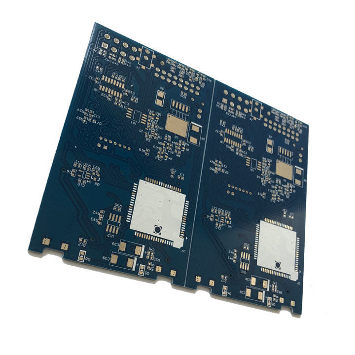
Laser Drill HDI FR4 PCB Board Fast Charger for 5G Multilayer 12 Layer
Linked Electronics is a professional pcb board manufacturer, providing PCB and PCBA with 2 decades experience. Our services includes
1)1-32 layers PCB board
2)HDI Blind&Buried via multilayers PCB board
3)High frequency special material base PCB board, like Rogers, Taconic, Arlon, etc.
4)Thick copper Technology, impedance control boards
5)Assembly Processing: SMT, COB, THT
6)Testing Methods: Flying Probe Test, X-ray, ICT and AOI.
HDI PCB is defined as a printed circuit board with a higher wiring density per unit area than conventional PCB. They have finer lines and spaces, smaller vias and capture pads and higher connection pad density than employed in conventional PCB technology. It is now widely used in communication PCB boards, which allows more components on a limited PCB area. Beside it will enable components to be assembled on both sides. The product size will geting smaller and lighter.
Why Linked Electronics for your HDI PCB fabriciation
Quality
Our UL/Rohs standards insure quality assemblies from start to finish. Whether it's a simple custom product or a complex turnkey production run, Linked will adhere to the highest quality standards all the time
Capable
Linked offers the latest in assembly capabilities and qualifications insuring that quality is built into every product we produce.
Experience
When it comes to your build you want a partner you can depend on. Our management team has over 10years of combined industry knowledge. Our engineering team has over 8 years experience.
Protecting your interests
Protecting your Intellectual Property is job one! Our staff colleague of trained professionals are all working under a strict confidentiality contract and treat your important documentation as they would their own.
Flexibility
Linked Electronics prides ourselves on our ability to custom tailor programs around our customers' needs. We are always happy to hear feedbacks from our customers.
Product type: 6-layer gold plate
Application: Automative
Special features:
Dyne value ≥38dyn
Press-fit hole

| CAPABILITY |
STANDARD |
ADVANCED |
| MinimumLayer Count |
1 |
1 |
| Maximum Layer Count |
12 |
32 |
| Material |
FR-4 (Tg-135C, 145C, 170C), Halogen- free
Rogers Ultralam 2000, Rogers RO4350, Rogers RO4003
Polyimide
Teflon
Black FR-4
Arlon AR-350
CEM-3
Getek Copper Clad Thermal Substrates
Hybrid (Rogers and FR4) BT Epoxy
Nelco 4013
PTFE
Metal Core Materials
Aluminum Core
|
| Board Thickness |
0.020"-0.125" |
0.005"-0.250" |
| Maximum Board Size |
16" x 22"
12" x 21"
22" x 28"
|
10" x 16"
16" x 22"
12" x 21"
22" x 28"
|
| Copper Thickness |
0.5 oz – 3 oz |
0.25 oz – 12 oz |
| Minimum Trace Width / Spacing |
0.004"/0.004" |
0.003"/0.003" |
| Solder Mask Color |
Green, Blue, Black, Red, Yellow, White, Clear, and customized |
| Silkscreen Color |
White, Black, Yellow, Green, Red, Blue and customized |
| Minimum Hole Size |
0.008" |
0.004" |
| Finished Hole Size Tolerance |
+/-0.003" |
+/-0.002" |
| PCB Surface Finish |
HASL (vertical & Horizontal), Lead Free HASL, OSP/Entek, ENIG, ENEPIG,
HASL + Gold Finger,Immersion Tin(ISn), Immersion Silver(IAg), Carbon
Ink, Hard Gold(Flash Gold), Soft Gold
|
| IPC Class |
Class 2 |
Class 3 |
| Controlled Impedance Tolerance |
+/-10 % |
+/-5 % |
| Blind Vias |
Yes |
Yes |
| Buried Vias |
Yes |
Yes |
| Aspect Ratio |
8/1 |
15/1 |
| Minimum Core Thickness |
0.004" |
0.002" |
| Carbon Ink |
Yes |
Yes |
| Peelable Mask |
Yes |
Yes |
| Solder Sample |
Yes |
Yes |
| First Article |
Yes |
Yes |
| ISO 9001: 2008 |
Yes |
Yes |
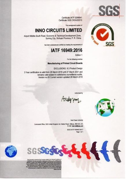
| ISO/TS16949: 2009 |
Yes |
Yes |
| UL 94v0 |
Yes |
Yes |
Logistics Information
Linked Electronics is not only trying to give customers a good product but also pay attention to offering a complete and safe package. And here we prepare some personalized services for all the orders.
Common packaging:
PCB: Sealed bag, Anti-static bags, Suitable carton.
PCBA: Antistatic foam bags, Anti-static bags, Suitable carton.
Regular Cartons Specification.
| Regular Cartons Specification |
No. Dimension (L*W*H) |
| Small Size |
33cm*28.5cm*18.5cm |
| Medium Size |
44.5cm*30cm*15cm |
| Big Size |
51.5cm*32.5cm*17.5cm |
Customized Cartons:
Outside of the carton a label will be made according to the requirements of customers printed the name of the customer address, mark, the customer needs to specify the destination and other information.
 Your message must be between 20-3,000 characters!