FR4 PCB Board Expedite Service by Linkd Electronics HASL Lead Free PCB Prototypes
Based in Shenzhen China, Linked electronics specialize in PCB manufacturing, PCB assembly, and component sourcing services.
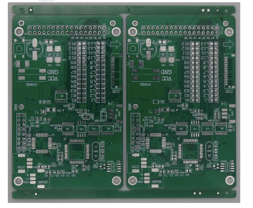
Our PCB fabrication service includes FR4 PCBs, Aluminum PCBs, HDI PCBs, Multilayer PCBs (up to 32 layers), Gold Finger PCBs and Rogers PCBs manufacturing
There are three reasons to buy PCBs from Linked Electronics
1. Superb and consistent Quality
2. Prices you will not find elsewhere
3. Knowledgable and personal Service
If you care about cost of your printed circuit boards, but you cannot afford to compromise quality, you have landed in the right place and you need look no further!
We specialise in small to medium volume runs - and we welcome prototypes.
Does your company need a high quality finished PCB shipped in
3 Days? 2 Days? Even 24 Hours?
Just email us and we are ready to help you.
FAQ
1: Does Linked accept small order for PCB fabrication
Yes, we specialized in prototype PCBs, you can order 1pcs from us. And we are happy to
assist you.
2: Is Linked a trading company or factory?
Linked is a factory with strong engineering team who can help customers to do ODM & OEM PCBA one stop service since 1998.
3: How to customized a sample?
Send us your PCB spec including PCB thickness, copper weight, soldermask and silkprint color, surface treatment and other requirements if any.
4: Do I need to pay deposit for an order?
For sampling or small led pcba order, Linked usually requires 100% full payment before shipping. For bulk order, 50% deposit with order, the balance was paid before delivery
PCB Manufacturing Capability by Linked Electronics
| Item |
Capability |
Remark |
| Layer count |
2~30 layer |
|
| Lamination |
FR-4,Aluminum Based,Copper based,High frequency plate,Heavy copper,BT,Rogers,PTFE ect |
|
| Thickness (THK) |
0.2mm≤THK≤6.0mm |
|
| Smallest hole (mm) |
0.15mm |
|
| Aspect Ratio |
13:1 |
|
| Max dimension |
Single or 2-layer |
600 x 1000 mm |
|
| Multi-lyr |
≤6L |
600 x 900 mm |
|
| ≥8L |
500 x 600 mm |
|
| Gold THK |
Hard Gold (u") |
50u" |
|
| Immersion Gold (u") |
4u" |
|
| Copper THK |
Outer (oz) |
6oz |
|
| Inner (oz) |
6oz |
|
| Smallest trace width / space (mil) |
3/3 mil |
|
| Annual ring |
Via hole |
3mil |
|
| Component hole |
6mil |
|
| Copper to edge spacing |
0.25mm |
|
| Min trace width / space (mil) |
Base Copper (oz) |
Min trace width / space (mil) |
|
| 0.5 |
3/3 |
| 1 |
4/4 |
| 2 |
5/5 |
| 3 |
7/7 |
| 5 |
9/9 |
Logistics
Our PCBs can reach all over the world in just 2 working days. If you need expedite service, our UPS
can reach some place in North America and Europe in just 1 working days.

 Your message must be between 20-3,000 characters!