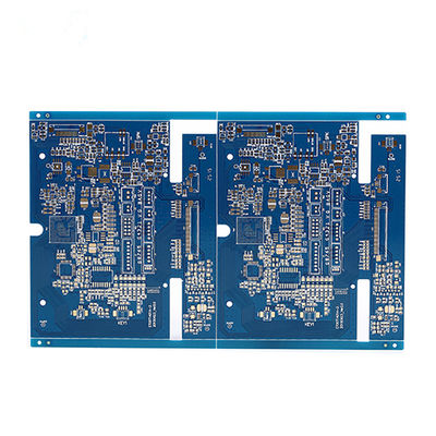
Multilayer 0.8mm FR4 BGA PCB Board 35um Copper All Layers ENIG Gold
About us
Lined Electronics Shenzhen OEM PCB Assembly Manufacturing
Linked Electronics is Electronic PCB & PCBA manufacturer
Specifications:
1.Fast and one-stop service
2.Accept PCB design,clone and OEM/ODM service.
3.PCB+Components+PCBA
4.Quote within 48 hours for PCBA projects and 2 hours for PCB fabrication projects
Founded back in 1998, Linked Electronics has been doing a great job in PCB and PCBA manufacturing for more than 2 decades now. We have very high capabilties for the production of double sided electronic PCB board, aluminum PCB board, multilayer FR4 PCB board, PCB assembly, SMT and DIP. Our main PCB business is for small and low volume PCB and PCBA production.
Our good service, on time delivery and excellent quality has help us win great reputation among our customers. Contact Linked Electronics today, and we look forward to seeing you.

PCB Capabilities
| Standard |
IPC Class2/IPC Class3 |
√ |
Products&
Manufacture |
Available laminate |
FR-4 High TG material
Halogen free FR-4
FR-1,CEM-1, Aluminum base |
| |
PCB Maximum Layer |
64 |
| |
Board Thickness |
0.2mm to 7mm |
| |
Min. Track Width/Space |
2mils/2mils |
| |
Min. Annular Ring |
3mils |
| |
Min. finished hole size |
4mils/0.1mm
|
| |
Copper thickness |
0.5oz to 20oz |
| |
Impedance control |
+/-10% |
| Surface Finishing |
Lead Solder HASL |
√ |
| |
Lead-Free Solder LF HASL |
√ |
| |
Immersion Gold/ENIG |
√ |
| |
Immersion Silver |
√ |
| |
Immersion Tin |
√ |
| |
OSP |
√ |
| |
Carbon Priting |
√ |
| |
Gold finger |
√ |
| Outline Profiling |
CNC Routing |
√ |
| |
V-Groove |
√ |
| |
Punching |
√ |
| |
Edge Plating |
√ |
| File Format |
GERBER |
√ |
| |
PROTEL 99SE |
√ |
| |
PROTEL DXP |
√ |
| |
POWER PCB |
√ |
| |
CAM350 |
√ |
| |
GCCAM |
√ |
| |
ODB+(.TGZ) |
√ |
PCB Process

BGA PCB Board
BGA, ball grid array (BGA), is a kind of surface-mount packaging which is used for IC. BGA packages, generally use on the microprocessors. A BGA can provide more interconnection pins than can be put on a dual in-line or flat package, each pin is provided with a solder ball. All connections are distributed in a uniform surface grid or matrix on the component. The whole bottom surface of the device can be used instead of just the perimeter. The leads are also on average shorter than with a perimeter-only type, leading to better performance at high speeds. Soldering of BGA devices requires precise control and is usually soldered by automated SMT production line.
The BGA component looks like

The BGA component on a PCB design Looks like the following

BGA under X-ray Test

Cold Solder Joints

Advantages of BGA Packages:
High Interconnection density
Takes less space on PCB Solder balls used along with stencils will self-align and give great ease to soldering technician while soldering BGA ICs
Low Thermal Resistance of BGA IC package due to efficient heat transfer from heat sinks, heat spreaders and good thermal contact using thermal paste to dissipate heat more effectively. Wide space between pads allows easy soldering. The lower signal inductance and impedance is controlled by separate ground and power planes.
Good electrical conductivity due to shorter interconnection between PCB pad and die. No broken or bent pins like any other leaded package like QFN The BGA packages have larger solder pads that makes the BGA package to be easily de-soldered and rework. Reduced thickness of BGA package render it useful in mobile phones. BGA based PCBs are highly cost effective
 Your message must be between 20-3,000 characters!
 Please check your E-mail!
  Your message must be between 20-3,000 characters!
 Please check your E-mail!


