


![]()
|
|
|
SMT Definition
Surface-mount technology (SMT) is a method in which the components or ICs are mounted directly onto the surface of a printed circuit board (PCB). An electrical component mounted in this manner is referred to as a surface-mount device (SMD). In industry, this approach has largely replaced the through-hole technology construction method of fitting components, the main reason is that SMT allows for increased manufacturing automation. Both technologies can be used on the same board, with the through-hole technology often used for components not suitable for surface mounting such as large transformers and heat-sinked power semiconductors.
The Advantages of SMT Technology in PCB Designs.
The important advantage of SMT in manufacturing includes reduced board cost, reduced material handling costs, and a controlled manufacturing process. Routing of traces is reduced, the size of the board is reduced, and number of drilled holes are also reduced
|
Product Details:
Payment & Shipping Terms:
|
| Product Name: | SMT PCB Board | Place Of Origin: | Shenzhen, China |
|---|---|---|---|
| Soldermask: | Green | Silkprint: | Black Legend |
| Application: | Industrial IoT | Size: | 100mm*230mm |
| High Light: | smt pcba,smt printed circuit board assembly |
||
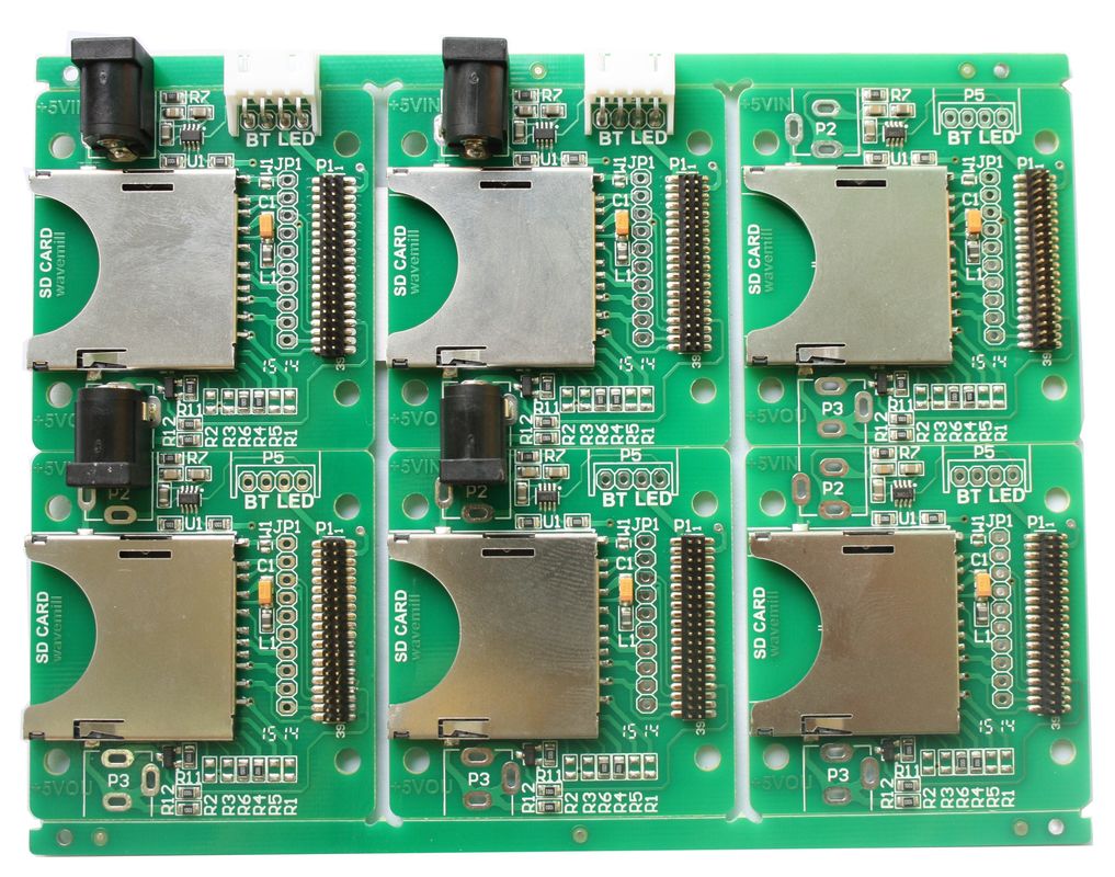
Rohs Electronic Customized PCB Board SMT/Assembly/DIP Service 4 Layer
What can Linked Electronics do for you?
![]()
Linked Electronics is PCB manufacture in China which supports PCB fabrication from prototypes, small volume to mass production. And without MOQ, you can order even 1pcs at Linked PCB. PCBs produced at Linked are widely used in the following applications LED products, communication equipments, industry control products, automotive, aerospace and Bluetooth etc.
Why choose Linked Electronics for your PCB Production?
![]()
PCBA Introduction
| Quantity | Prototype&Low Volume PCB Assembly,from 1 Board to 250,is specialty,or up to 1000 |
| Type of Assembly | SMT,Thru-hole |
| Solder Type | Water Soluble Solder Paste,Leaded and Lead-Free |
| Components |
Passive Down to 0201 size BGA and VFBGA Leadless Chip Carriers/CSP Double-sided SMT Assembly Fine Pitch to 0.8mils BGA Repair and Reball Part Removal and Replacement |
| Bare Board Size | Smallest:0.25*0.25 inches Largest:20*20 inches |
| File Formate | Bill of Materials Gerber files Pick-N-Place file |
| Types of Service | Turn-key,partial turn-key or consignment |
| Component packaging | Cut Tape,Tube,Reels,Loose Parts |
| Turn Time | Same day service to 15 days service |
| Testing | Flying Probe Test,X-ray Inspection AOI Test |
| PCB assembly process | Drilling-----Exposure-----Plating-----Etaching & Stripping-----Punching-----Electrical Testing-----SMT-----Wave Soldering-----Assembling-----ICT-----Function Testing-----Temperature & Humidity Testing |
PCB Capability at Linked Electronics
| PCB TECHNOLOGIES | STANDARD | PROTOTYPE | ADVANCED (HDI) |
| Up to 20 Layers | Yes | Yes | Yes |
| Blind and Buried Vias | Yes | Yes | Yes |
| Sequential lamination | Yes | Yes | Yes |
| Impedance Control | Yes | Yes | Yes |
| Hybrids And Mixed Dielectrics | Yes | Yes | Yes |
| Aluminum Core PCBs | Yes | Yes | Yes |
| Via In Pad | Yes | Yes | Yes |
| Conductive Hole Fill | Yes | Yes | Yes |
| Edge Plating And constellation Holes | Yes | Yes | Yes |
![]()
Contact Person: Mr. Jonathan
Tel: +86 755 2553 8256
Fax: 86-755-61658416