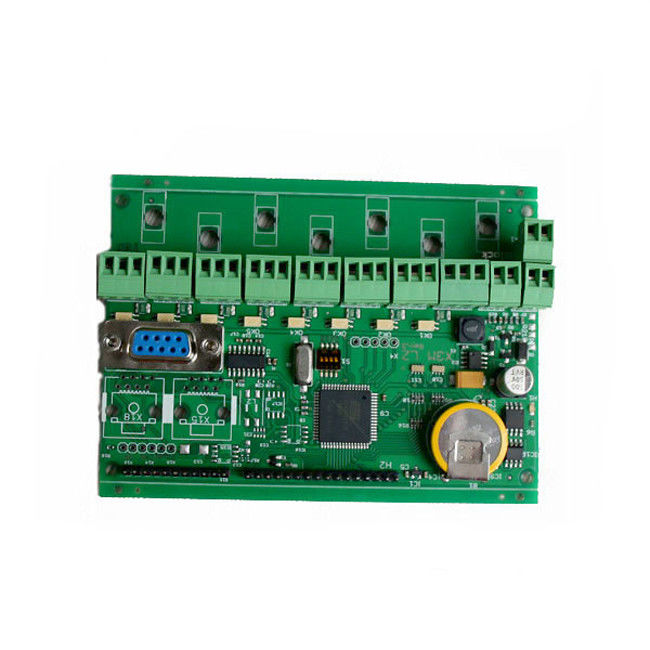
Electronic PCB Board Assembly Gold Finger Printed Circuit Board FR4 2.4mm
Electronic PCB Board Assembly Gold Finger Printed Circuit Board FR4 2.4mm
Linked Electronics is a one stop PCB solution provider. We offer services for PCB, FPC, PCB assembly, PCB SMT, Components sourcing and laser stencils.
If you have any PCB boards to be produced, get us the gerbers files, BOM, pick and places files. Our salesteam will get back to you asap.
| Item |
Capability |
| 1.Base Material |
FR-4 / High TG FR-4 / Halogen Free material/Rogers/Arlon/Taconic/Teflon |
| 2.Layers |
1-32 Layers |
| 3.Finised inner/outer copper thickness |
1-6OZ |
| 4.Finished board thickness |
0.2-7.0mm |
| 7.Min hole size |
Mechanical hole: 0.15mm Laser hole: 0.1mm |
| 9.Controlled Impedance |
+/-5% |
| 13.Plugging vias capability |
0.2-0.8mm |
| 15.Outline profile |
Rout/ V-cut/ Bridge/ Stamp hole |
| 16.Surface treatment |
HASL, HASL lead free, Immersion Gold, Immersion Tin, Immersion Silver, Hard gold, Flash gold, OSP…
|
Providing one stop PCB service, we have customers around the world. We use cutting-edge technology to provide time-critical product to communications, aerospace, defense, IT, medical equipment, precision test equipment and industrial control companies and manufacturers. And our good service, quality wins us great reputation among customers.

We know how important environment and continuous developemt is to us. Linked Electronics is committed to a clean, safe and healthy environment. Caring for the environment is one of our core corporate values and we strive for continuous improvements. Linked is also committed to comply with all the environmental laws and regulations. With our employees working together, these actions benefit customers, shareholders, employees, our community and our planet.
FAQ
Q: What files does Linked Electronics needed for PCBA service?
A: Gerber or Eagle, BOM listing, pick and place files, 3D picture ( if you have) and a picture of last
version boards.
Q:Is it possible that a sample be offered by Linked Electronics.
A: Yes, we can custom you sample to test before mass production
Q: When will I get the quotation after sent Gerber, BOM and test procedure?
A: Within hours for PCB quotation and 2 working days for PCBA quotation.
Q: How can I know the process of my PCBA production?
A: 7-10 working days for PCB production and components purchasing, and 10 working days for PCB assembly and Testing
Q: How can I make sure the quality of my PCBAs?
A: We ensure that each piece of PCBA products work well before shipping. We'll test all of them according to your test procedure. Also if there are any defect items during the shipping, free repaire work can be offered.
Q: Do I need to pay deposit for an order?
A: For sampling or small led pcba order, Linked usually requires 100% full payment before shipping. For bulk order, 50% deposit with order, the balance was paid before delivery
PCB Products Show
 Your message must be between 20-3,000 characters!