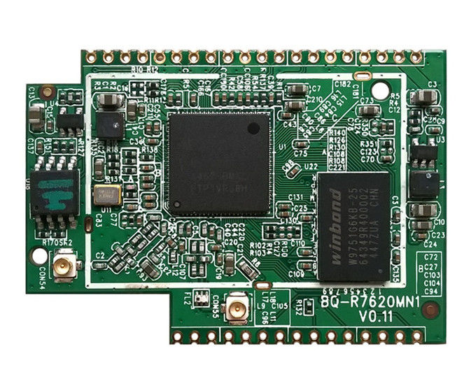
Multilayer Electronic PCB Board Assembly 4 Layer 1OZ HASL Lead Free
Linked electronics was established in 1998 in Shenzhen, as one of the leading PCB manufacturers in China, is dedicated to provide high-tech PCB products. Our PCB fabrication service includes FR4 PCBs, Aluminum PCBs, HDI PCBs, Multilayer PCBs (up to 32 layers), Gold Finger PCBs and Rogers PCBs manufacturing.
At Linked Electronics, we can provide electronic manufacturing from design, rapid prototyping to medium volume manufacturing. Our team is highly skilled to react to all our customer demands and we pride ourselves on high standards of quality along with excellent delivery performance.
There is no order too small for us, we offer 1-piece board with 1-day assembly lead time. And Linked guarantees an on-time delivery of rapid PCB assembly service.
Contact us Linked Electronics today, and let's discuss your PCB demand.
Linked Electronics Provides Following One-Stop PCB Services
1. PCB design , ODM service.
2. Schematic design and Layout
3. Fast PCB&PCBA prototype and Mass Production
4. Electronic Components Sourcing Services
5. PCB Assembly Services:SMT,DIP&THT,BGA repair and reballing
6. ICT, Constant Temperature Burn-in and Function Test
7. Stencil,Cables and Enclosure building
8. Standard Packing and On time Delivery

| 1 |
Description |
PCB Specification |
| 2 |
Material |
FR-4/HIGH TG150-180 FR-4/CEM-1/CEM-3/Aluminum |
| 3 |
Layer |
1-32 |
| 4 |
Board Thickness |
0.2mm- 4.0mm |
| 5 |
Board Thickness Tolerance |
+/-10% |
| 6 |
Copper thickness |
17.5um-175um (0.5oz-5oz) |
| 7 |
Min Trace Width |
0.15mm |
| 8 |
Min Space Width |
0.15mm |
| 9 |
Min Drilling Dia |
0.2mm |
| 10 |
PTH copper thickness |
0.4-2mil(10-50um) |
| 11 |
Tolerance of Etching |
±1mil(±25um) |
| 12 |
V-cut angle |
25°,30°,45°,60° |
| 13 |
Pearl Strength of line |
≥ 6lb/in(≥ 107g/mm) |
| 14 |
Impedance control and tolerance |
50Ω±10% |
| 15 |
Twist&Wrap |
≤ 0.5% |
| 16 |
Soldermask |
Green, Red, Blue, White, Black, Yellow |
| 17 |
Surface Finish/Plating |
HASL/Lead Free HASL/OSP/Gold Plating/Immersion Gold/ENIG |
| 18 |
Certificate |
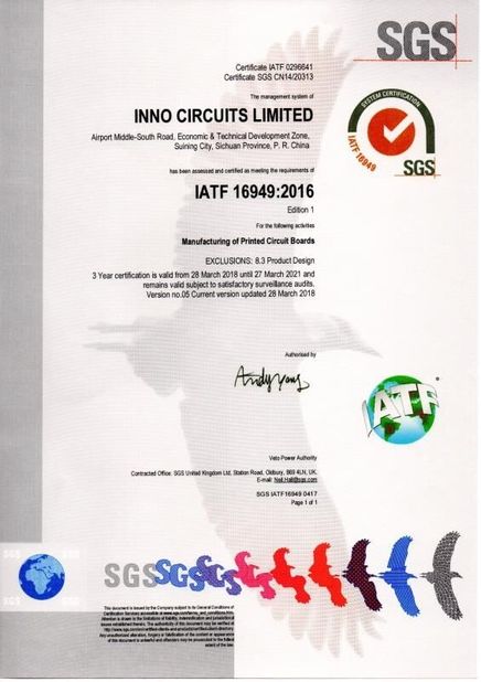
ROHS. ISO9001 |
| 19 |
File |
Protel 99se/P-CAD/Autocad/Cam350 |
| 20 |
Inner packing |
Vacuum packing,Plastic bag |
| 21 |
Outer packing |
Standard carton packing |
PCB or PCB Assembly files requests
1. Gerber files of the bare PCB board
2. BOM (Bill of material) for assembly, pick and place files
3. Testing Guide & Test Fixtures if necessary
4. Programming files & Programming tool if necessary
Envrionmental Policy
Linked staff love the planet that we live, and we know how important it means to us.
We focus on clean production and enviromental protection the day when Linked is founded.
1.Manage energy within the organisation, including the design of our products and facilities.
2. Be committed to complying with relevant legislation including those affecting packaging, waste disposal and emissions and other requirements to which we subscribe.
3. Reduce the consumption of materials and promote re-cycling and the use of re-cycled materials.
4.Promote environmental awareness and responsibility amongst all stakeholders we can influence.
5. Set environmental objectives and targets and regularly monitor and review our progress towards achieving them.
6. Communicate to all persons working for or on behalf of the organisation.
 Your message must be between 20-3,000 characters!