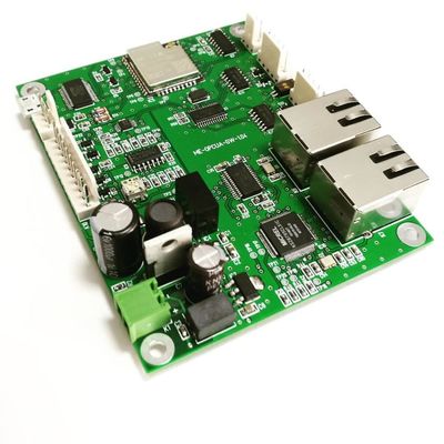
Custom Electronic PCB Assembly for Monitor Instruments PCB Board SMT
Welcome to Linked Electronics( One stop PCB solution service provider)
Our company story
We started Linked Electronics because we were tired of the poor customer service and board quality from other PCB companies. We knew that we could do better. We always do our best to exceed our customer's expectations by providing exceptional personal customer service and competitively priced high-quality PCBs that are delivered on time.
We love engineers.
We do everything in our power to help engineers to make AWESOME THINGS. We understand the importance of delivering on our promises and that is why, each day, smart engineers from around the world rely on us to manufacture their mission-critical printed circuit boards.
Features
1. Fast quotes.
2. Quick turn delivery. Same day turn available on two layer PCB, 48hour turn on multilayer PCB.
3. Copper weight 1 oz to 6 oz
4. Available finishes include HASL, Lead free HASL, Nickel/Gold, soft bondable gold, ENIG, ENEPIG, immersion Tin, immersion Silver, Carbon Ink,and more
5. In inventory materials include FR4, Rogers Alumium, Polymide.
6. Prototype to full production PCB.
PCB Assembly Service Capability
| Item |
Lot Size |
| Normal |
Special |
Remark |
| PCB(used for SMT)spec |
(L*W) |
Min |
L≥50mm |
L<50mm |
Includes the Process Edge |
| W≥50mm |
| Max |
L≤460mm |
L > 460mm |
| W≤400mm |
W> 400mm |
| (Thickness) |
Min thickness |
0.5mm |
T<0.5mm |
| Max thickness |
4.5mm |
T>4.5mm |
| SMT components spec. |
dimension |
Min size |
201 |
1005 |
/ |
| (0.6mm*0.3mm) |
(0.3mm*0.2mm) |
| Max size |
200mm*125mm |
200mm*125mm<SMD |
/ |
| component thickness |
T≤6.5mm |
6.5mm<T≤15mm |
/ |
| QFP,SOP,SOJ(multipins) |
Min pin space |
0.4mm |
0.3mm≤Pitch<0.4mm |
/ |
| CSP,BGA |
Min ball space |
0.5mm |
0.3mm≤Pitch<0.5mm |
/ |
| |
|
|
|
|
|
| Item |
Prototype Manufacturer |
| Normal |
Special |
Remark |
| SMT PCB SPEC |
(L*W) |
Min size |
L≥50mm |
L<50mm |
Includes the Process Edge |
| W≥30mm |
| Max size |
L≤450mm |
L:800-450mm |
| W≤350mm |
W:400-350mm |
| (Thickness) |
Minimum thickness |
0.8mm |
T<0.8mm |
| Maximum Thickness |
2mm |
T>2mm |
| DIP PCB SPEC |
(L*W) |
Min Size |
L≥50mm |
L<50mm |
| W≥30mm |
| Max Size |
L≤500mm |
L≥500mm |
| W≤300mm |
W≥300mm |
| (Thickness) |
Minimum Thickness |
0.8mm |
T<0.8mm |
| Maximum Thickness |
2mm |
T>2mm
|
On Time Delivery
We have maintained a consistent on time shipping record that our partners have come to rely on. If at all possible, we are now actually shipping many orders early! We are strategically located a few miles away from Hongkong Internation Airport in order to ship our items faster than other competitors.
Delivery precision solutions to fit your production needs

EXPRESS: 24 h – X days
Quick turn for some PCBs could be 24 hours when there’s a very urgent demand. When short lead times are required we use our factories that specialise in fast turn-round and send the PCBs by express direct airfreight.

COST-EFFICIENT STANDARD FREIGHT: 4 – 6 weeks
Optimum time/cost ratio is calculated on capacity, technology, volume and freight mode.

CLIMATE-SMART FREIGHT: 8 – 12 weeks
Transportation efficiency is a major environmental factor to consider. As a result, we offer sea freight and sea-air as options. These options are more environment-friendly and also reduce the total freight costs. However, it will be 6 weeks more for sea freight. Our recommendation is only to use this mode of freighting for major volumes and PCBs of fairly low added value. Climate-smart freight is also advised where our customer offers an environmentally-certified product and must be able to provide environmental accounting for all components of the production process.
PCB industries / markets Linked Electronics Serves
 Industrial, Automotive, and Commercial: With over 2 decades of PCB expertise, we have a huge array of customers that are leaders in their commercial and industrial niches. With our high-technology PCB capabilities, we have created long-lasting partnerships throughout various industrial and commercial niches.
 Medical and Bio-medical: When strict quality standards are required, various niche medical device companies and medical equipment OEM manufacturers depend on us for their medical PCB and PCBA manufacturing.
 Students and Hobbyist: With our straightforward and no hidden cost PCB pricing, we have earned the trust of multiple educational institutions from around the world. When students need affordable printed circuit boards for their various university projects, they rely on Linked Electronics.
 Your message must be between 20-3,000 characters!
 Please check your E-mail!
  Your message must be between 20-3,000 characters!
 Please check your E-mail!


