SMT PCB Assembly LED Display Controller Quick Turn PCB Fabrication
Linked Electronics is a leading Printed Circuit Board manufacturer and PCB assembly manufacture in China, offering one stop PCB solution service. Quick Turn turnaround Prototype Circuit Boards are our speciality. 2 Layer PCB could be finished in 12 hours.
Linked One Stop PCB Service
1. PCB manufacturing
2. Components Souring
3. PCB Assembly Service
Look forward to your RFQs and hope we can work together.
FAQs
Q1.What is needed for PCB PCBA quotation?
· PCB: Gerber file or other PCB files and Spec for the boards (material,surface finish treatment, copper thickness,board thickness,Quantity ,...)
· PCBA: PCB file, BOM, Pick and Place Files
Q2. What file formats do you accept for PCB PCBA production?
· Gerber file: CAM350 RS274X Format
· PCB file: Protel 99SE, P-CAD 2001 PCB, Eagle, Altium
· BOM: Excel (PDF,word,txt)
Q3. NDA?
NDA can be signed. You will be assured that your files will NOT sent to any third party. We protect the intellectual property for our customers in the whole process.
Q4. What’s the MOQ?
Linked Electronics don’t have any minimum lot requirements, so you never have to buy more than what you need.
.
PCBA Capabilty
| Item |
Lot Size |
| Normal |
Special |
Remark |
| PCB(used for SMT)spec |
(L*W) |
Min |
L≥50mm |
L<50mm |
Includes the Process Edge |
| W≥50mm |
| Max |
L≤460mm |
L > 460mm |
| W≤400mm |
W> 400mm |
| (Thickness) |
Min thickness |
0.5mm |
T<0.5mm |
| Max thickness |
4.5mm |
T>4.5mm |
| SMT components spec. |
dimension |
Min size |
201 |
1005 |
/ |
| (0.6mm*0.3mm) |
(0.3mm*0.2mm) |
| Max size |
200mm*125mm |
200mm*125mm<SMD |
/ |
| component thickness |
T≤6.5mm |
6.5mm<T≤15mm |
/ |
| QFP,SOP,SOJ(multipins) |
Min pin space |
0.4mm |
0.3mm≤Pitch<0.4mm |
/ |
| CSP,BGA |
Min ball space |
0.5mm |
0.3mm≤Pitch<0.5mm |
/ |
| |
|
|
|
|
|
| Item |
Prototype Manufacturer |
| Normal |
Special |
Remark |
| SMT PCB SPEC |
(L*W) |
Min size |
L≥50mm |
L<50mm |
Includes the Process Edge |
| W≥30mm |
| Max size |
L≤450mm |
L:800-450mm |
| W≤350mm |
W:400-350mm |
| (Thickness) |
Minimum thickness |
0.8mm |
T<0.8mm |
| Maximum Thickness |
2mm |
T>2mm |
| DIP PCB SPEC |
(L*W) |
Min Size |
L≥50mm |
L<50mm |
| W≥30mm |
| Max Size |
L≤500mm |
L≥500mm |
| W≤300mm |
W≥300mm |
| (Thickness) |
Minimum Thickness |
0.8mm |
T<0.8mm |
| Maximum Thickness |
2mm |
T>2mm |
Quality Gurantee
100%Electrical Test
IPC-6012A Qualification and Performance Specification for Rigid Printed Boards
IPC-A-600G Acceptability of Printed Boards
PERFAG 2E,3C
CUL Certificated Standard for Printed Boards
Rohs Compliance
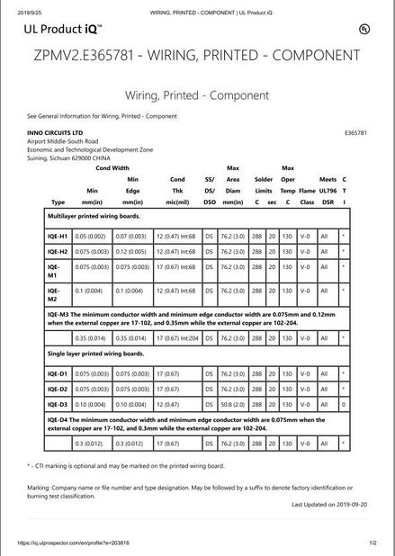
UL796 Standard for Safety Printed Wiring Board
ISO14001:2004
ISO TS16949:2009
ISO9001(2008)
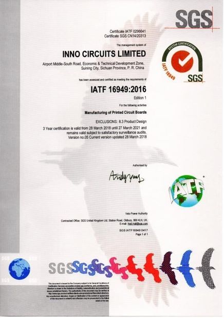
SGS audited supplier certificate
PCBA Packing by Linked Electronics
 Your message must be between 20-3,000 characters!