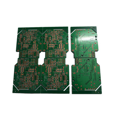
HDI PCB Board Multilayer Circuit Board 6 Layer HASL Rohs Gold Finger SMT Available
Linked Electronics is a China company with a legacy of precision, economy and efficiency.
The 20+ years in service has secured Linked a strong foundation of long standing valued clients.
Their legacy has delivered its diverse services to such Industries as Electronics, Government, Gaming and Communication to name just a few.
That's 20+ years of operation with 20+ years of staff commitment.
Linked is a company you can rely on. Look forward to your RFQs.
Service that Linked is Able to Provide
Printed Circuit Boards
Linked Electronics specializes in higher layer count PCBs, exotic materials, laser drill micro-vias, blind/buried vias, as well as conductive and non-conductive via fill.
PCB Assembly
Linked Electronics. is your expert in PCB fabrication & Assembly for:
• Prototypes
• Medium Volumes
• Large Batch Volumes
Using your design, we orient individual parts on the PCBs and solder the assemblies together, returning finished PCBs to you.
For assembly only, you provide all the parts needed for the project; we provide the labor.
• For Partial Turn-Key assembly, you provide what you can; we obtain the rest of the parts and then provide the labor.
• For Full Turn-Key assemblies, you only need to provide the design; we obtain all parts including the bare PCBs and provide all labor.
To ensure precision and repeated installation, parts are placed by machine and then soldered, using the appropriate reflow or wave process.
Testing
At Linked, we employ appropriate testing methods to make sure that everything is properly assembled according to your plans, and we inspect the finished product.
Standard Lead time
| Layer Count |
Lead time |
|
| |
S< 1㎡ |
1㎡≤S< 3㎡ |
3㎡≤S< 5㎡ |
5㎡≤S< 10㎡ |
10㎡≤S< 30㎡ |
|
| 2L |
5 |
7 |
9 |
11 |
13 |
|
| 4L |
6 |
8 |
10 |
12 |
14 |
|
| 6L |
7 |
9 |
11 |
14 |
15 |
|
| 8L |
8 |
10 |
12 |
15 |
16 |
|
| 10L |
9 |
12 |
14 |
16 |
17 |
|
| 12L |
10 |
13 |
15 |
17 |
18 |
|
Service Flow

 Your message must be between 20-3,000 characters!
 Please check your E-mail!
  Your message must be between 20-3,000 characters!
 Please check your E-mail!


