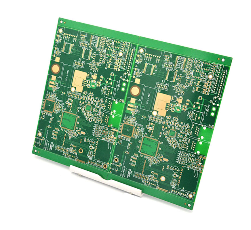
OEM HDI PCB Board Micro Drill 0.1mm HDI Electronic Circuit Board Lead Free
Linked Electronics is an OEM manufacturer that focus on PCB&PCBA manufacturing over 20 years. We can manufacture pcb ranging from basic single sided boards up to 32 layers ,and provide one stop turnkey services, including PCB manufacture, assembly, components source , function testing services etc.
HDI PCB Circuit Board Description
| PCB Name |
HDI PCB |
| The number of layers |
2~32 Layer |
| Material |
FR4,AL |
| The finished copper thickness |
1~6OZ |
| Solder mask color |
customized |
| Silkscreen |
customized |
| Surface treatment |
customized |
FAQ
Q1.What is needed for PCB or PCBA quotation?
· PCB: Gerber file or other PCB files and Spec (material,surface finish treatment, copper thickness,board thickness,Quantity ,...)
· PCBA: PCB file, BOM, Pick and Place Files
Q2. What file formats do you accept for PCB PCBA production?
· Gerber file: CAM350 RS274X Format
· PCB file: Protel 99SE, P-CAD 2001 PCB, Eagle, Altium
· BOM: Excel (PDF,word,txt)
Q3. What’s the MOQ?
Linked Electronics don’t have any minimum lot requirements, so you never have to buy more than what you need.
Q4. Will you discose the file to any other people.
NDA can be signed. Your files will NOT sent to any third party. We protect the intellectual property for our customers in the whole process.
Linked Electronics' Advantages
1. One Stop Contract Manufacturing
2. Quick Turn, Prototypes can be finished in 12hours
3. Prefessional engineering team which will view the gerber carefully before production
4. No MOQ you will never order more than you want at Linked Electronics
5. Quick Respone, you will always receive our reply in 2 working hours
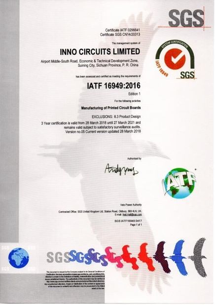
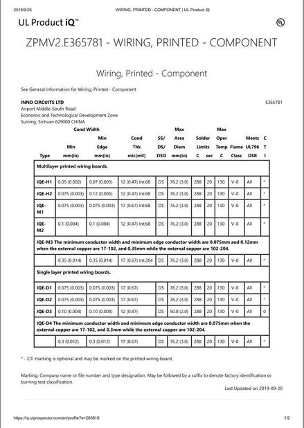
6. UL, TS16949 Certified Manufacturing

PCB Process Flow
 Your message must be between 20-3,000 characters!