Customized HDI PCB Board Multilayer PCB ENIG Surface Treatment RF Application
Linked Electronics is an OEM manufacturer that focus on PCB&PCBA manufacturing over 20 years. We can manufacture pcb ranging from basic single sided boards up to 32 layers ,and provide one stop turnkey services, including PCB manufacture, assembly, components source , function testing services etc.
HDI PCB Circuit Board Description
| Layer: 12 Layer |
Mini Hole: 0.15mm |
| Material: FR4 TG130 Kingboard |
Mini Width/space: 4mil/6mil |
| Thickness: 1.6 mm |
Testing points:1089 |
| Copper thickness: 35um |
Solder Mask: Dark Green |
| Finish:ENIG Rohs |
Silkscreen: White |
You can obtain price quote from our website, or contact us by sales@linked-elec.com
As a part of our constant efforts toward improvement, we welcome your feedback.
Linked Electronics. is all about delivering your PCB and PCB assemblies on time, and providing excellent quality. We appreciate your business, and look forward to serving you.
Linked Electronics' Advantages
1. One Stop Contract Manufacturing
2. Quick Turn, Prototypes can be finished in 12hours
3. Prefessional engineering team which will view the gerber carefully before production
4. No MOQ you will never order more than you want at Linked Electronics
5. Quick Respone, you will always receive our reply in 2 working hours
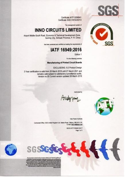
6. UL, TS16949 Certified Manufacturing

Enviromental Policy
Linked Electronics continues to focus on environmental protection and clean production, take actions to protect surroundings, and strictly abide by international and domestic conventions and requirements. We have had a sophisticated environmental protection facilities system, which can control pollutants effectively.
Water Disposal Instruments
 Your message must be between 20-3,000 characters!