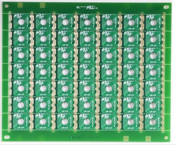
Shenzhen OEM Quick Turn PCB Electronic PCB and PCBA Assembly
Welcome to Linked Electronics.Linked has been in business for 2 decades specializing in quick turn, high quality custom PCB fabrication.
Linked can meet all your PCB requirements, from Single-Sided (SS) to Double-Sided (DS-PTH) to complex Multi-Layer (ML) – up to 32 layers. We also do Flexible, Flexi-Rigid and Metal Core (Aluminium and Copper Alloy) Circuits.
PCB Specification
| Product Name |
Electronic Custom PCB Printed Circuit Board PCBA Design |
| Type |
Rigid |
| Material |
FR4, CEM1, CEM3, High Frequency Board, |
| Layer |
1,2,4,6...32 Layer |
| Shape |
Rectangular, Round, Slots, Cutouts, Complex, Irregular |
| Cutting |
Shear, V-score, Tab-routed |
| Board Thickness |
0.2-6mm, regular 1.6mm |
| Copper Thickness |
0.5-4oz, regular 1oz |
| Solder Mask |
Green, Red, Blue, Yellow, etc. |
| Silk Screen |
White, Black, etc. |
| Silk Screen Min Line Width |
0.006" or 0.15mm |
| Min Trace/Gap |
0.1mm or 4mils |
| Min Drill Hole Diameter |
0.01",0.25mm or 10mils |
| Surface Finish |
HASL Rohs, ENIG, OSP, etc. |
FAQs
1, What service do you have?
We provide turnkey solution including PCB fabrication, SMT, plastic injection & metal,final assembly, testing and other value-added service.
2, What is needed for PCB & PCBA quotation?
For PCB: Quantity, Gerber file and technic requirements(material,size, surface finish treatment, copper thickness,board thickness).
For PCBA: PCB information, BOM,Testing documents.
3, How to keep our product information and design file secret ?
We are willing to sign a NDA effect by customers side local law and promising to keep customers data in high confidential level.
4, What are the main products of your PCB/PCBA services?
Automotive, Medical, Industry Control,IOT,Smart Home etc
5, What is your minimum order quantity (MOQ)?
Our MOQ is 1 PCS, sample and mass production is available
Our Environmental Policy
Linked Electronics is committed to conducting its business in an environmentally responsible manner.
Linked Electronics will comply with all international and local environmental laws and regulations applicable to its operations. We will manage its activities to prevent environmental pollution; will introduce “green” materials and “pollution-free” facilities/technologies in its operation to minimize the effects of its products and production process to the environment.

 Your message must be between 20-3,000 characters!