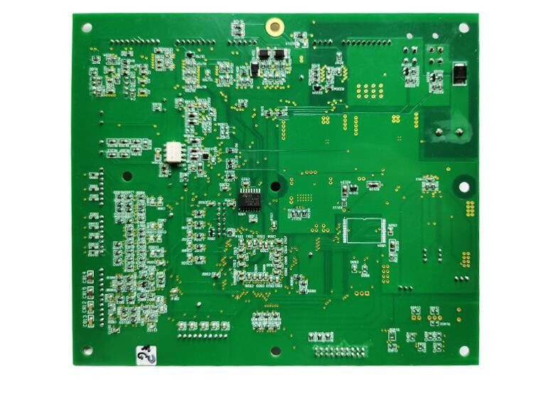
Quick Turn PCB with Good Quality Lead Free PCB Assembly Prototype PCBA
Welcome to Linked Electronics, manufacture of printed circuit boards prototypes. Linked has been serving high mix, low volume and quick turn PCB for more than 20 years.
If you are interested, just email us and let's discuss in detail.
Standard Lead time
| Layer Count |
Lead time |
|
| |
S< 1㎡ |
1㎡≤S< 3㎡ |
3㎡≤S< 5㎡ |
5㎡≤S< 10㎡ |
10㎡≤S< 30㎡ |
|
| 2L |
5 |
7 |
9 |
11 |
13 |
|
| 4L |
6 |
8 |
10 |
12 |
14 |
|
| 6L |
7 |
9 |
11 |
14 |
15 |
|
| 8L |
8 |
10 |
12 |
15 |
16 |
|
| 10L |
9 |
12 |
14 |
16 |
17 |
|
| 12L |
10 |
13 |
15 |
17 |
18 |
|
| |
|
|
|
|
|
|
Quick turn for 2 layer prototype could be finished in 12 hours
FAQ
Q1.What is needed for PCB PCBA quotation?
· PCB: Gerber files other PCB files and Spec (material,surface finish treatment, copper thickness,board thickness,Quantity etc)
· PCBA: PCB file, BOM, Pick and Place Files
Q2. What file formats do you accept for PCB PCBA production?
· Gerber file: CAM350 RS274X Format
· PCB file: Protel 99SE, P-CAD 2001 PCB, Eagle, Altium
· BOM: Excel (PDF,word,txt)
Q3. NDA?
NDA can be signed. Your files will NOT sent to any third party. We protect the intellectual property for our customers in the whole process.
Q4. What’s the MOQ?
Linked Electronics don’t have any minimum order quantity, so you never have to buy more than what you need.
Raw Material Supplier
We have a good relationship with our main suppliers. All the raw material suppliers are the top
supplier in the industry.

Main Equipment
 Your message must be between 20-3,000 characters!